- 您现在的位置:买卖IC网 > Sheet目录117004 > 534AB000187BGR (SILICON LABORATORIES) CRYSTAL OSCILLATOR, CLOCK, 850 MHz, LVPECL OUTPUT
Si534
Rev. 1.0
9
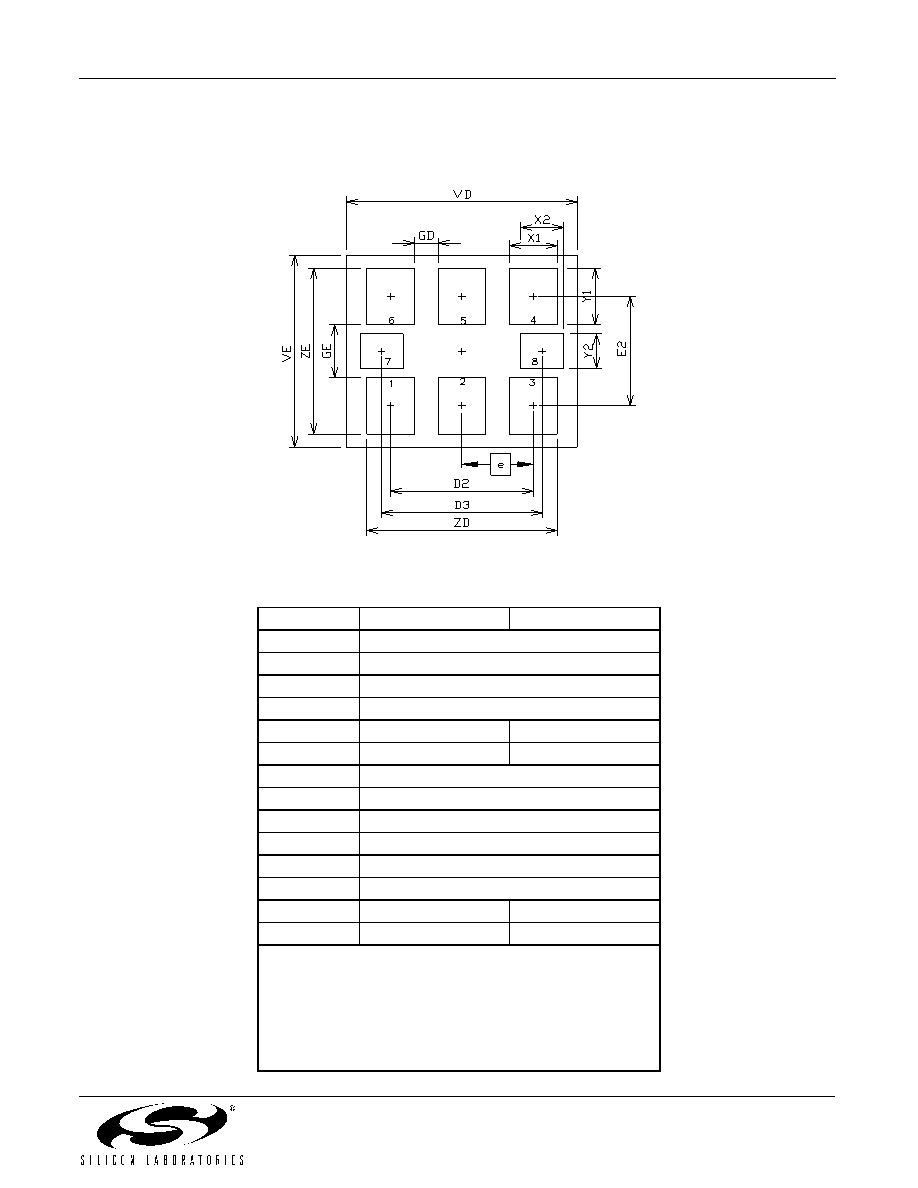
5. 8-Pin PCB Land Pattern
Figure 3 illustrates the 8-pin PCB land pattern for the Si554. Table 11 lists the values for the dimensions shown in
the illustration.
Figure 3. Si534 PCB Land Pattern
Table 11. PCB Land Pettern Dimensions (mm)
Dimension
Min
Max
D2
5.08 REF
D3
5.705 REF
e
2.54 BSC
E2
4.20 REF
GD
0.84
—
GE
2.00
—
VD
8.20 REF
VE
7.30 REF
X1
1.70 TYP
X2
1.545 TYP
Y1
2.15 REF
Y2
1.3 REF
ZD
—
6.78
ZE
—
6.30
Note:
1. Dimensioning and tolerancing per the ANSI Y14.5M-1994
specification.
2. Land pattern design follows IPC-7351 guidelines.
3. All dimensions shown are at maximum material condition
(MMC).
4. Controlling dimension is in millimeters (mm).
发布紧急采购,3分钟左右您将得到回复。
相关PDF资料
534CB000016BG
CRYSTAL OSCILLATOR, CLOCK, 74.25 MHz, CMOS OUTPUT
534CB000154BGR
CRYSTAL OSCILLATOR, CLOCK, 45.8752 MHz, CMOS OUTPUT
530HC982M000DGR
CRYSTAL OSCILLATOR, CLOCK, 982 MHz, CMOS/TTL OUTPUT
530JA119M000DG
CRYSTAL OSCILLATOR, CLOCK, 119 MHz, CMOS OUTPUT
530NA870M000DGR
CRYSTAL OSCILLATOR, CLOCK, 870 MHz, LVDS OUTPUT
530CB32M0000BGR
CRYSTAL OSCILLATOR, CLOCK, 32 MHz, CMOS OUTPUT
531FA388M000DG
CRYSTAL OSCILLATOR, CLOCK, 388 MHz, LVDS OUTPUT
531BB273M000DGR
CRYSTAL OSCILLATOR, CLOCK, 273 MHz, LVDS OUTPUT
相关代理商/技术参数
534AB000240DG
制造商:Silicon Laboratories Inc 功能描述:SMD CRYSTAL OSC 450MHZ/580MHZ/625MHZ/640MHZ 3.3V 6PIN - Trays
534AB000287DG
制造商:Silicon Laboratories Inc 功能描述:SMD CRYSTAL OSC 850MHZ/900MHZ/940MHZ/1GHZ 3.3V 6PIN - Trays
534AB000287DGR
制造商:Silicon Laboratories Inc 功能描述:SMD CRYSTAL OSC 850MHZ/900MHZ/940MHZ/1GHZ 3.3V 6PIN - Tape and Reel
534AB000289DG
制造商:Silicon Laboratories Inc 功能描述:SMD CRYSTAL OSC 155.52MHZ/161.13281MHZ/167.331712MHZ/173.370 - Trays
534AB000289DGR
制造商:Silicon Laboratories Inc 功能描述:SMD CRYSTAL OSC 155.52MHZ/161.13281MHZ/167.331712MHZ/173.370 - Tape and Reel
534AB000298DG
制造商:Silicon Laboratories Inc 功能描述:SMD CRYSTAL OSCILLATOR 155.52MHZ/156.25MHZ/161.13281MHZ/166. - Trays
534AB000305DGR
制造商:Silicon Laboratories Inc 功能描述:SMD CRYSTAL OSC 10MHZ/16.384MHZ/22.5792MHZ/24.576MHZ 3.3V 6P - Tape and Reel
534AB000334DG
制造商:Silicon Laboratories Inc 功能描述:SMD CRYSTAL OSC 167.33172MHZ/173.37078MHZ/644.53125MHZ/657.4 - Trays